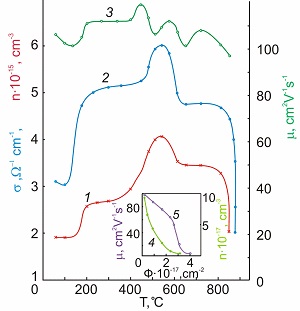
• When the defect concentration excesses some critical value, defects of new kind with a strong scattering field are formed
• High temperature annealing of the irradiated sample with increased vacancy concentration causes the appearance of the vacancy emptiness with the lower electron density
• Increase of the defects’ concentration might be the reason of the qualitative changes of electrical properties in irradiated crystal as well as increase of the diffusion processes intensity during high temperature annealing
Semiconductor Physics, Quantum Electronics & Optoelectronics, 21 (2), P. 130-133 (2018).
DOI: https://doi.org/10.15407/spqeo21.02.130
Self-organization in irradiated semiconductor crystals caused by
thermal annealing
M. Zavada1, O. Konoreva1, P. Lytovchenko1, V. Opilat2, M. Pinkovska1, O. Radkevych3, V. Tartachnyk1
1Institute for Nuclear Research, NAS of Ukraine, 47, prospect Nauky, 03028 Kyiv, Ukraine
2Taras Shevchenko National University of Kyiv, 64/13, Volodymyrska Str., 01601 Kyiv, Ukraine
3SE "SRI of Microdevices" STC "Institute for Single Cristals", NAS of Ukraine,
3, Pivnichno-Syretska str., 04136 Kyiv, Ukraine
Corresponding author: phone +38(044)-525-37-49; e-mail: okskon@meta.ua
Abstract. Annealing of complex semiconductors GaP and CdP 2 , irradiated at room temperature by high fluences of electrons within 1…30 MeV energy interval and 80 MeV α -particles, was carried out and main electrical parameters (conductivity σ, carrier concentration n and mobility µ) as well as the positron life-time τ were studied and analyzed. When the point defect concentration excesses some critical value, defects of new kind are formed: oscillation peaks in the isochronous annealing curve appear, and defects with a high cross-section of defect scattering and capture are created. High temperature annealing of the irradiated sample with increased vacancy concentration causes appearance of the vacancy voids with a lower electron density.
Keywords: gallium phosphate, defects, electron irradiation, self-organization, annealing.

This work is licensed under a Creative Commons Attribution-NoDerivatives 4.0 International License.