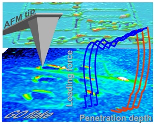
Combined mechanical scanning probe lithography approach has been applied for the direct mask-less modification of graphene oxide (GO) flakes and the mask patterns engraving in layers of chalcogenide resist with a nanometer scale resolution. It could be used for the lab-level device prototyping, developing the functional prototypes of new devices in bio/nanosensorics, plasmonics, 2D electronics and other modern technology branches.
Semiconductor Physics, Quantum Electronics & Optoelectronics, 21 (2), P. 152-159 (2018).
DOI: https://doi.org/10.15407/spqeo21.02.152
Features of mechanical scanning probe lithography on graphene oxide and As(Ge)Se chalcogenide resist
P.M. Lytvyn1, S.V. Malyuta2, I.Z. Indutnyi1, A.A. Efremov1, O.V. Slobodyan2, V.I. Min’ko1, A.N. Nazarov2, O.V. Borysov2, I.V. Prokopenko1
1V. Lashkaryov Institute of Semiconductor Physics,
41, prospect Nauky, 03680 Kyiv, Ukraine,
E-mail: plyt@isp.kiev.ua
2National Technical University of Ukraine “Igor Sikorsky KPI”,
37, prospect Peremohy, 03056 Kyiv, Ukraine,
E-mail: serhiy.malyuta@gmail.com
Abstract. Combined mechanical scanning probe lithography (SPL) approach applied for the direct mask-less modification of graphene oxide (GO) flakes and the mask patterns engraving in layers of chalcogenide resist with a nanometer scale resolution have been implemented in this work. It was compared the dynamics of mechanical modification of chalcogenide films and multilayer GO flakes deposited from an aqueous suspension. The double-layer As40Se60/As4Ge30S66 chalcogenide resist developed for mechanical SPL and pattern formation processes have optimized. The resist with the thickness close to 100 nm provides the formation of minimal pattern elements with the size of several tens nanometers. The SPL approach was realized on the basis of serial NanoScope IIIa Dimension 3000TM scanning probe microscope, and original software utilities were developed. These mechanical SPL could be intended for the verification of innovative ideas in academic researches, the laboratory-level device prototyping, developing of functional prototypes of new devices in bio/nanosensorics, plasmonics, 2D electronics and other modern technology branches.
Keywords: mechanical scanning probe lithography, graphene oxide, chalcogenide semiconductor glass, atomic force microscopy.

This work is licensed under a Creative Commons Attribution-NoDerivatives 4.0 International License.